The intricate dance of electrons, the precision of miniaturized components – at the heart of nearly every modern electronic device lies an Integrated Circuit (IC) board. Mastering The IC Board Design Process Workflow isn't just about connecting dots; it's about engineering the nervous system of tomorrow's technology. It's where innovation meets meticulous execution, where a flawless design can launch a groundbreaking product, and a single oversight can send a project back to square one. This guide will walk you through the essential stages, principles, and tools, transforming complex concepts into a clear, actionable blueprint for success.
At a Glance: Your Blueprint for IC Board Design Success
- Foundation First: Understand the core components – ICs, resistors, capacitors, inductors – and their roles.
- Structured Lifecycle: Follow a six-stage workflow from requirements to manufacturing, ensuring systematic development.
- Key Principles: Master signal integrity, power integrity, thermal management, EMC, and DFM for robust designs.
- Essential Tools: Leverage EDA software like Altium Designer or Cadence, alongside hardware tools for verification.
- Strategic Choices: Know when to opt for traditional IC board design versus System-in-Package (SiP).
- Future-Proofing: Stay ahead with insights into AI in EDA, advanced packaging, and flexible PCBs.
- Learn from Examples: Grasp real-world challenges and solutions through practical case studies.
The Foundation: What Makes an IC Board Tick?
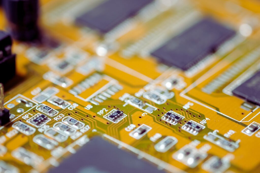
Before diving into the process, let's establish a clear understanding of what an IC board is and its fundamental building blocks. At its core, IC board design is the art and science of arranging electronic components—especially Integrated Circuits (ICs)—and their intricate interconnections onto a Printed Circuit Board (PCB). Think of it as creating a high-rise city for electrons, where every street (trace), building (component), and power grid must be perfectly orchestrated to ensure seamless operation. These boards are the unsung heroes inside everything from your smartphone to life-saving medical equipment.
The efficacy of an electronic system hinges on these boards, making their design a critical discipline. To grasp the design workflow, you first need to be acquainted with the primary residents of this electronic city:
- Integrated Circuits (ICs): The Brains: These are miniaturized electronic circuits etched onto a single semiconductor chip. Packed with millions or even billions of transistors, capacitors, and resistors, ICs act as the control centers of a device, like the CPU in your computer. They process information, execute commands, and orchestrate the overall functionality.
- Resistors: The Traffic Cops: These components control the flow of electric current by providing resistance. They are crucial for limiting current in specific parts of a circuit, dividing voltage, and ensuring components receive the right amount of power.
- Capacitors: The Energy储能大师: Capacitors store and release electrical energy. They are often used for filtering electrical noise, smoothing out DC voltage fluctuations, or timing circuits. Imagine them as tiny, fast-charging batteries that deliver quick bursts of energy when needed.
- Inductors: The Magnetic Guardians: Coils of wire that store energy in a magnetic field, inductors are typically used to block high-frequency signals while allowing low-frequency signals to pass through. You'll commonly find them in RF (Radio Frequency) circuits, acting as filters or chokes.
Together, these components form a complex yet harmonious ecosystem, each playing a vital role in the board's overall function.
The Blueprint for Success: Navigating The IC Board Design Process Workflow
Executing an IC board design is a journey, not a sprint. It's a systematic workflow, broken down into six interconnected stages, each demanding precision and foresight. Skipping a step or rushing through a phase can lead to costly errors and delays down the line.
Stage 1: Decoding the Vision — Requirement Analysis
Every great design begins with a clear understanding of what needs to be achieved. Requirement analysis is the foundational stage where you define the functional, performance, physical, and cost objectives of your board. This isn't just about technical specifications; it incorporates market research, anticipates customer needs, and sets the non-negotiable parameters for the entire project.
Key Questions to Answer:
- What is the device supposed to do (e.g., process data, capture images, transmit signals)?
- How fast, efficient, or accurate does it need to be (e.g., processing speed, battery life, signal-to-noise ratio)?
- What are the physical constraints (e.g., size, weight, environmental durability)?
- What's the target manufacturing cost and budget?
This stage sets the stage for everything that follows, guiding component selection, shaping circuit topology, and defining how different modules will interface. Without a solid requirements document, you're building in the dark.
Stage 2: Bringing Ideas to Life — Schematic Design
With requirements firmly in hand, you translate that vision into a detailed electrical blueprint: the schematic. This stage involves using sophisticated Electronic Design Automation (EDA) tools like Altium Designer, OrCAD, or KiCad to create a diagram that visually represents all components and their electrical connections.
Here, you'll select specific ICs, resistors, capacitors, and other parts, then connect them with lines representing electrical pathways. Beyond simple drawing, schematic design includes critical tasks:
- Component Placement: Placing symbols for each part on the schematic sheet.
- Electrical Connections: Defining all necessary wire connections between component pins.
- Net Labeling: Assigning unique names to electrical nets for clarity and organization.
- Electrical Rule Checks (ERC): Automated checks to identify potential short circuits, open circuits, or other fundamental electrical errors.
- Functional Simulations: Running virtual tests to verify the circuit's behavior under various conditions before committing to a physical layout.
The schematic is the brain of your design; it dictates how electricity flows and how the components will interact. A well-executed schematic simplifies subsequent stages significantly.
Stage 3: Laying the Groundwork — PCB Layout
Now, the abstract connections from your schematic begin to take physical form. PCB layout is where you physically arrange all the components onto the board's surface. This is a highly iterative and critical stage, directly impacting performance, manufacturability, and cost.
Critical Considerations:
- Component Placement Optimization: Not just about fitting parts, but positioning them strategically. High-speed signals benefit from shorter trace lengths, while heat-generating components (like powerful ICs) need to be near ventilation or heat sinks to prevent overheating.
- Thermal Management: Proactive placement to dissipate heat efficiently, preventing performance degradation and extending component lifespan.
- Electromagnetic Compatibility (EMC): Shielding sensitive components, creating proper ground planes, and ensuring sufficient spacing to prevent interference between components and with the external environment. This also helps in guarding against Electrostatic Discharge (ESD).
The layout phase is where the physical reality of your design starts to emerge. Every millimeter counts, influencing everything from signal integrity to the ultimate size and cost of the product.
Stage 4: Weaving the Connections — Routing
Once components are placed, the routing stage commences: drawing the copper traces (the "wires" on the PCB) that electrically connect them according to your schematic. This is far more than drawing lines; it's a highly complex task governed by strict electrical and manufacturing rules.
Key Aspects of Routing:
- Electrical Rule Adherence: Following guidelines for minimum trace width (for current capacity), clearance (preventing shorts), and maximum length (for signal integrity).
- Signal Integrity (SI): Maintaining the quality of electrical signals. This involves techniques like impedance matching, minimizing reflections, and reducing crosstalk (where signals interfere with adjacent traces). For high-speed designs, this is paramount.
- Power Stability (PI): Ensuring a clean, stable power delivery to all components, often achieved through dedicated power planes and decoupling capacitors.
- Multi-layer PCBs: For complex designs, routing is done across multiple copper layers, interconnected by vias (small drilled holes). Strategic layer stack-up is crucial for managing signal integrity and power distribution.
Effective routing transforms a static component arrangement into a dynamic, functional circuit. It requires a deep understanding of electrical physics and meticulous attention to detail.
Stage 5: Proving the Concept — Simulation and Verification
Before committing to costly manufacturing, you rigorously test your design in a virtual environment. Simulation and verification are about catching potential flaws and optimizing performance without cutting a single piece of copper.
This stage involves a suite of analyses:
- Electrical Simulations:
- Signal Integrity (SI) analysis: Checking for signal distortion, reflections, overshoot, undershoot, and crosstalk on high-speed lines.
- Power Integrity (PI) analysis: Verifying stable power delivery, identifying voltage drops, and analyzing noise on power planes.
- Electromagnetic Interference (EMI) analysis: Predicting potential electromagnetic radiation and susceptibility issues.
- Thermal Simulations: Analyzing heat distribution across the board to identify hot spots and ensure components operate within safe temperature limits.
- Mechanical Simulations: Assessing physical stress, vibration resistance, and overall structural integrity, especially for boards in harsh environments.
- Design Rule Checks (DRC): Automated checks (within EDA software) against a comprehensive set of manufacturing and electrical design guidelines, ensuring the design can actually be built.
Simulation and verification are your last line of defense against design errors, saving immense time and money by preventing costly redesigns after prototyping.
Stage 6: From Digital to Tangible — Manufacturing and Testing
The final stage brings your digital design into the physical world. Manufacturing involves a series of precise steps:
- Gerber File Generation: Converting your digital design into a set of standardized files that instruct manufacturing machines.
- Etching and Drilling: Removing unwanted copper to create traces and drilling holes for vias and component leads.
- Plating: Adding copper to drilled holes to create electrical connections between layers.
- Solder Mask Application: Applying a protective layer that prevents solder bridges and shorts.
- Silkscreen Printing: Adding labels, reference designators, and logos for assembly and identification.
Once the bare PCB is fabricated, components are assembled onto it using either Surface-Mount Technology (SMT) for high-density, automated placement, or Through-Hole Technology (THT) for larger, more robust components.
Finally, the assembled boards undergo rigorous testing: - Electrical Checks: Testing for shorts, opens, and correct component values.
- Functional Verification: Powering up the board and testing its actual performance against the original requirements. This might involve running firmware, connecting to external devices, and measuring outputs.
This comprehensive approach ensures that the manufactured board not only physically matches the design but also performs as intended, paving the way for mass production. Learn more about IC board design to deepen your understanding of these foundational elements.
Mastering the Fundamentals: Pillars of Robust IC Board Design
Beyond the sequential workflow, several fundamental principles underpin every successful IC board design. Neglecting any of these can lead to unreliable performance, manufacturing headaches, and even product failure.
Signal Integrity: The Purity of Communication
Signal integrity (SI) is about ensuring that electrical signals transmit accurately from one point to another without distortion, attenuation, or interference. In high-speed circuits, issues like impedance mismatch and crosstalk can wreak havoc on signal quality, leading to:
- Reflections: Signals bouncing back due to impedance changes.
- Overshoots/Undershoots: Voltage exceeding or falling below expected levels.
- Ringing: Oscillations caused by reflections.
- Crosstalk: Interference between adjacent signal traces.
Key Techniques for SI: - Impedance Control: Matching trace width, spacing, and dielectric material to control the characteristic impedance.
- Impedance-Matching Components: Using series resistors or termination resistors.
- Minimizing Trace Length: Shorter traces reduce opportunities for signal degradation.
- Differential Signaling: Using two traces with opposite polarity signals to reduce noise and improve noise immunity.
Power Integrity: The Unwavering Current
Power integrity (PI) guarantees a stable and clean power supply to all components. Fluctuations, noise, or voltage drops in the power delivery network (PDN) can severely impact component performance, introduce errors, and even cause system crashes.
Elements of a Robust PDN:
- Low Impedance: Designing the PDN (power planes, vias) to have very low impedance across a wide frequency range.
- Power Noise Reduction: Strategically placing decoupling capacitors close to ICs to supply instantaneous current and filter out high-frequency noise.
- Proper Grounding: A solid ground plane is crucial for stable reference voltages and return paths for current.
Thermal Management: Keeping Cool Under Pressure
Excessive heat is the enemy of electronics. Thermal management prevents components from overheating, which can degrade performance, reduce lifespan, and cause catastrophic failures.
Effective Thermal Strategies:
- Strategic Component Placement: Positioning heat-generating components near cooling mechanisms (heat sinks, fans) or where airflow is optimal.
- Thermal Vias: Small, plated holes that conduct heat away from components into ground or power planes, which act as heat spreaders.
- Copper Pours: Large areas of copper on the PCB to spread heat away from hot spots.
- Dedicated Heat Sinks and Fans: External solutions for high-power devices.
Electromagnetic Compatibility (EMC): Peaceful Coexistence
EMC ensures that your board functions correctly within its electromagnetic environment without generating undue interference (EMI) or being susceptible to external electromagnetic phenomena (EMS). This is crucial for regulatory compliance and reliable operation.
Achieving EMC:
- Shielding: Enclosing sensitive components or entire sections of the board with conductive materials.
- Proper Grounding: A unified, low-impedance ground plane minimizes noise and provides a stable reference.
- Filtering: Using capacitors and inductors to block unwanted noise on power and signal lines.
- ESD Protection: Designing circuits to withstand Electrostatic Discharge events, which can be highly destructive.
Design for Manufacturability (DFM): Building with the End in Mind
DFM means designing your board with the manufacturing process in mind from the outset. This isn't just about making it work; it's about making it cost-effective, high-quality, and easy to produce at scale.
DFM Considerations:
- Manufacturing Tolerances: Adhering to the capabilities and limitations of your chosen fabricator.
- Component Placement for Assembly: Ensuring enough space for pick-and-place machines and soldering processes.
- Optimized Component Selection: Choosing readily available, cost-effective components suitable for automated assembly.
- Panelization: Arranging multiple boards on a single panel to streamline production.
By integrating DFM principles, you reduce production costs, improve yield, and accelerate time-to-market.
Your Essential Toolkit: Powering the Design Process
Modern IC board design would be impossible without a sophisticated array of tools, both software and hardware. These tools automate complex tasks, allow for virtual prototyping, and provide crucial insights into performance.
Electronic Design Automation (EDA) Software
EDA software suites are the backbone of digital design, integrating schematic capture, PCB layout, and simulation capabilities.
- Altium Designer: A comprehensive, integrated platform renowned for its unified environment. It covers schematic design, PCB layout, and signal integrity analysis, with powerful 3D design features that help visualize the physical board. It's often chosen for its balance of features and user-friendliness for complex designs.
- Cadence Allegro: A professional-grade tool suite designed for the most complex, high-speed, and high-density designs. Allegro excels in advanced routing, constraint management, and collaborative design environments, making it a staple in large corporations and for cutting-edge electronics.
- OrCAD: A long-standing name in EDA, OrCAD is particularly known for its powerful simulation capabilities (AC, DC, transient analysis). It boasts a user-friendly interface that helps engineers perform detailed circuit analysis.
- KiCad: The leading free and open-source EDA suite. KiCad offers schematic capture, PCB layout, and 3D viewing, supported by a vibrant and active community. It's an excellent choice for hobbyists, educational purposes, and even professional projects where budget is a concern.
Beyond Software: Crucial Hardware Tools
While software simulates and designs, hardware tools are indispensable for debugging, verification, and testing physical prototypes.
- Oscilloscopes: These devices analyze electrical signal waveforms, allowing you to visualize amplitude, frequency, phase, and other characteristics. They are critical for debugging circuits, verifying signal integrity, and identifying unexpected electrical behavior.
- Logic Analyzers: When dealing with multiple digital signals (e.g., in microcontrollers or FPGAs), logic analyzers capture and display their timing relationships simultaneously. They are invaluable for debugging complex digital systems and communication protocols.
- Thermal Imagers: These cameras visualize temperature distribution across a powered-on board, instantly identifying overheating components or inadequate thermal pathways. They are essential for validating your thermal management strategies.
Strategic Choices: IC Board Design vs. System-in-Package (SiP)
While traditional IC board design remains prevalent, advancements have introduced alternative integration strategies, notably System-in-Package (SiP). Understanding the differences is crucial for selecting the right approach for your project.
| Feature | IC Board Design | System-in-Package (SiP) |
|---|---|---|
| Definition | Arranges multiple discrete components on a PCB. | Integrates multiple ICs and passive components into a single, compact package. |
| Integration Level | Moderate to High | Very High |
| Size | Larger, due to discrete components and longer traces. | Significantly smaller, reduced footprint. |
| Performance | Good, but longer signal paths can impact high-speed signals. | Improved, with shorter signal paths and better signal integrity. |
| Design Flexibility | High, easy to modify or swap components. | Limited; design is "locked" into the package. |
| Manufacturing Cost | Generally lower for low-to-medium volume production. | Higher initial cost, but can be cost-effective at high volumes. |
| Time-to-Market | Longer design cycles for complex, high-density PCBs. | Faster, as pre-designed, tested blocks are integrated. |
| Typical Use Cases | Industrial control systems, prototyping, small-scale production, large electronics. | Wearable devices, 5G communication, IoT, medical implants, space-constrained applications. |
| For projects demanding ultimate miniaturization, high performance in compact spaces, and faster integration of complex functions, SiP offers distinct advantages. However, for most applications where flexibility and lower non-recurring engineering costs are paramount, traditional IC board design remains the go-to solution. |
Understanding the Micro-World: A Glimpse into IC Chip Design
While this article focuses on the board design, it's helpful to understand that the "IC" in "IC Board" itself undergoes a rigorous design process. The IC design lifecycle is about creating the miniaturized chip that will eventually be mounted onto your PCB. This distinction is critical: you design with ICs, but you don't typically design the ICs themselves unless you're a semiconductor company.
Briefly, the IC design lifecycle involves:
- Requirements: Defining the chip's specific functionality, power consumption, speed, and cost.
- Architecture: Outlining the overall chip structure and high-level design goals.
- Micro-architecture: Breaking down the architecture into specific, manageable components like memory blocks, arithmetic units, and communication interfaces.
- Implementation (RTL Design & Physical Design):
- RTL (Register Transfer Level) Design: Defining data transfer and operations using Hardware Description Languages (HDLs) like VHDL or Verilog, followed by extensive simulations.
- Physical Design: Translating this abstract logic into actual physical components (gates, transistors) and their layout on a silicon wafer, including placement, routing, and clock tree synthesis.
- Bringup: Testing prototypes of the fabricated IC to identify and debug design flaws or manufacturing defects.
- Productization: Optimizing the IC for efficient mass production.
- Sustaining: Providing ongoing support, updates, and fixes throughout the IC's lifespan.
This complex process yields the sophisticated components that are the stars of your IC board design.
The Horizon: Future Trends Shaping IC Board Design
The world of electronics is constantly evolving, and IC board design is no exception. Several emerging trends are set to revolutionize how boards are conceived, developed, and manufactured.
AI in EDA: The Intelligent Co-Pilot
Artificial intelligence (AI) is increasingly being integrated into EDA tools, transforming the design process. AI can act as an intelligent co-pilot, offering:
- Automated Layout and Routing: AI algorithms can quickly generate optimized component placements and trace routes, significantly reducing design time.
- Intelligent Design Optimization: Suggesting adjustments to trace widths, clearances, or component positions for improved signal integrity, power integrity, or thermal performance.
- Failure Prediction: Proactively identifying potential issues, such as EMI hotspots or thermal bottlenecks, even before physical prototyping.
AI promises to accelerate design cycles, enhance design quality, and open new possibilities for complex systems.
Advanced Packaging Technologies: Beyond 2D
Traditional packaging places ICs side-by-side. Advanced packaging technologies are breaking this mold to achieve greater density and performance:
- 3D Packaging: Stacking multiple ICs vertically, often connected by through-silicon vias (TSVs). This dramatically reduces the board footprint, leads to shorter signal paths (improving speed and signal integrity), and allows for greater functionality in a smaller volume.
- Fan-out Packaging: An evolution of wafer-level packaging where electrical connections are routed outwards from the die's edge, allowing for higher pin counts and improved electrical performance. This is particularly beneficial for mobile and IoT devices where space is at a premium and high-speed data transfer is critical.
These technologies are enabling the miniaturization and performance leaps seen in modern smartphones and other compact, high-power devices.
Flexible and Stretchable PCBs: Electronics That Conform
Imagine electronics that bend, twist, and stretch. Flexible and stretchable PCBs are emerging as a game-changer for several applications:
- Wearable Devices: Offering comfort, seamless integration with clothing or the body, and accommodating natural body movements.
- Biomedical Electronics: Conforming to organs or complex anatomical shapes, allowing for less invasive medical devices and more precise monitoring.
While promising, these technologies present challenges in material selection, manufacturing processes optimized for deformable substrates, and ensuring long-term reliability under mechanical stress. However, the potential for truly integrated, comfortable, and unobtrusive electronics is immense.
Real-World Impact: Case Studies in Design Excellence
Theory is one thing; practical application is another. Let's look at how the principles and workflow discussed manifest in real-world scenarios.
High-Speed IC Board for Data Center Server
Challenge: Designing a server board capable of handling 10 Gbps data rates, requiring extreme signal integrity, managing significant power consumption from high-performance processors, and dissipating substantial heat in a confined space.
Solutions Implemented:
- Advanced EDA Simulations: Rigorous signal integrity (SI) and power integrity (PI) simulations were performed to model high-frequency behavior.
- Impedance-Controlled Traces: Precisely controlled trace widths and spacing on multi-layer PCBs to maintain consistent impedance for high-speed differential signals.
- Multi-layer Power Distribution Network (PDN): Utilizing dedicated power and ground planes with extensive decoupling capacitors to ensure stable power delivery and minimize noise.
- Thermal Vias and Heat Sinks: Strategic placement of thermal vias under hot components, paired with large copper pours and custom-designed heat sinks and active cooling solutions.
Results: The design achieved ultra-reliable data processing speed, stable power delivery under heavy load, and an extended component lifespan due to effective thermal management, critical for 24/7 server operation.
Miniaturized IC Board for a Wearable Device
Challenge: Creating a compact, lightweight board for a smartwatch that required maximum miniaturization, extremely low power consumption for long battery life, and seamless integration of multiple sensors (heart rate, accelerometer, GPS).
Solutions Implemented:
- System-in-Package (SiP) and High-Density Interconnect (HDI) Technology: Multiple ICs (processor, memory, wireless module) were integrated into a single SiP, and HDI PCBs with micro-vias were used to pack more functionality into a smaller area.
- Low-Power Components and Efficient Power Management: Selection of ultra-low-power ICs and a sophisticated power management integrated circuit (PMIC) with dynamic voltage scaling and power gating features.
- Custom Firmware and Shielding for Sensor Integration: Developed custom firmware to optimize sensor power usage and implemented precise shielding techniques to prevent electromagnetic interference between sensitive sensors in close proximity.
Results: The final product was a compact, lightweight design with significantly longer battery life and accurate sensor data, meeting the demands of a competitive wearable market.
Your Next Steps: Building a Future-Proof Design Strategy
Mastering The IC Board Design Process Workflow is a journey of continuous learning and adaptation. As electronics become more complex and miniaturized, the demands on designers will only increase. By internalizing the structured workflow, adhering to fundamental principles, and leveraging the right tools, you're not just designing boards; you're engineering the future.
To excel, cultivate a mindset of meticulous planning, thorough verification, and continuous improvement. Embrace the iterative nature of design, viewing each simulation and test as an opportunity to refine and perfect. Stay curious about emerging technologies like AI in EDA and advanced packaging, as they will undoubtedly shape the next generation of electronic marvels. The most successful designs are born from a deep understanding of the fundamentals, coupled with a keen eye on the horizon. Your blueprint for success in IC board design is now clearer; the only thing left is to start building.