Every time you interact with a smartphone, drive a car, or even brew a cup of coffee using a smart appliance, you're experiencing the intricate magic of modern electronics. At the very core of these devices lies a marvel of engineering: the IC board. Far more than just a green slab with components, IC board design is the art and science of connecting integrated circuits (ICs) and other electronic parts into a functional, reliable, and powerful system. It’s the invisible architect that dictates how fast, how small, and how smart our gadgets can be, literally powering innovation across every industry.
This super pillar hub will guide you through the fascinating world of IC board design, from its fundamental concepts to the advanced techniques shaping its future. Whether you're a budding engineer, a seasoned professional, or simply curious about what makes your favorite electronics tick, you’ll discover how thoughtful design translates into the seamless experiences we rely on daily.
The Heart of Modern Electronics: Understanding ICs and PCBs
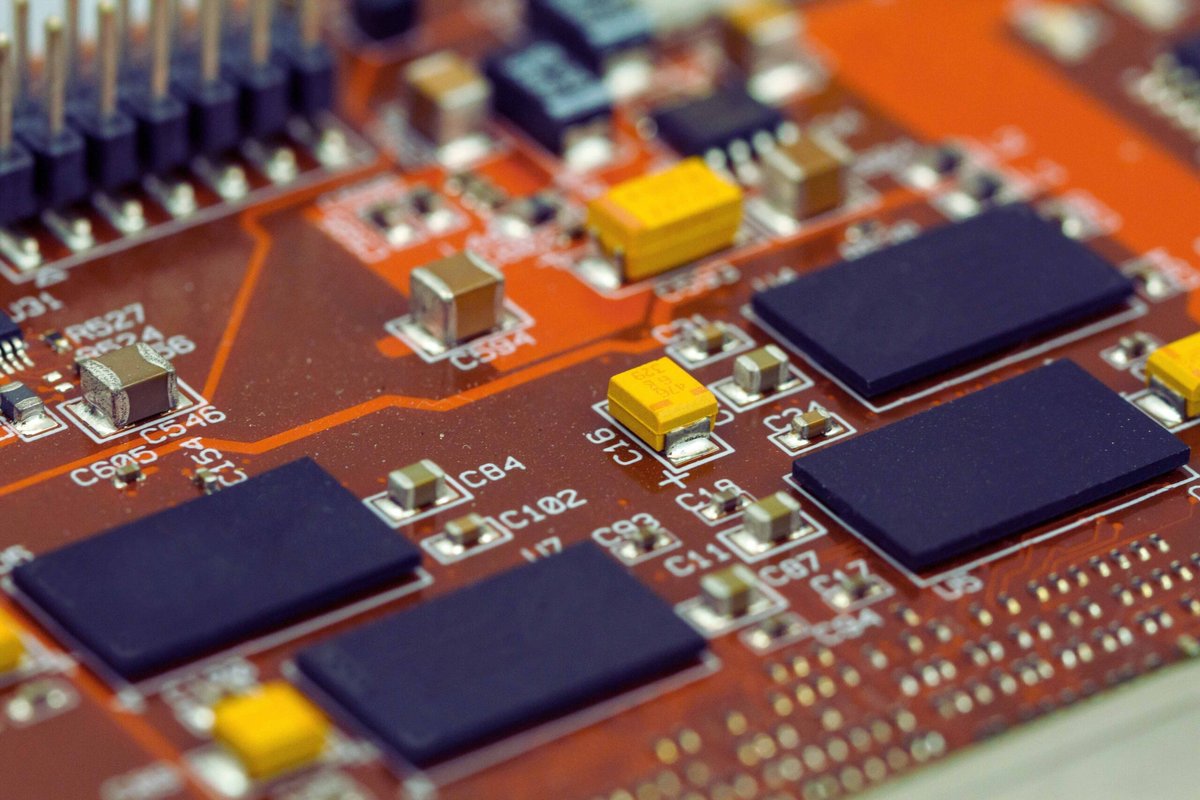
At the heart of any electronic device, two key elements work in concert: the Integrated Circuit (IC) and the Printed Circuit Board (PCB). An IC, often called a "chip," is a tiny semiconductor powerhouse, a miniature world etched onto a silicon wafer, housing millions or even billions of transistors, capacitors, and resistors. These sophisticated components perform the heavy lifting—from simple logic gates to complex microprocessors that serve as the brain of your device.
The PCB acts as the stage for these ICs and other supporting components. It’s a flat board made of non-conductive material, laminated with layers of copper traces that serve as electrical highways, allowing all the parts to communicate and function as a coherent system. The ICs themselves typically appear as small, often black, square or rectangular chips with numerous pins, which are soldered onto these copper traces. You can usually spot an IC by its unique part number printed on its surface.
IC board design then becomes the meticulous process of arranging these critical electronic components, with ICs at the forefront, and crafting their electrical interconnections onto a PCB to create a fully functional electronic system. Beyond the ICs, a functional board also relies on other vital components:
- Resistors: These control the flow of electrical current, ensuring components receive the correct amount.
- Capacitors: Acting like tiny batteries, they store and release electrical energy, smoothing out voltage and filtering unwanted noise.
- Inductors: Storing energy in a magnetic field, inductors are crucial for managing power and filtering specific frequencies.
Understanding how these core elements interact is the first step in appreciating the complexity and elegance of electronic systems. To truly grasp these foundational concepts and how they form the bedrock of every electronic device, we invite you to Explore IC board design fundamentals.
From Concept to Reality: The IC Board Design Process
The journey from an idea for a new electronic feature to a working IC board is a multi-faceted and highly structured process. It begins long before any physical board is ever laid out, starting with a clear vision of what the final product needs to achieve. Whether designing the IC itself or integrating existing ICs onto a new PCB, each stage demands precision and foresight.
The overarching design of an IC follows a rigorous path:
- Requirements Phase: Defining precisely what the IC needs to do, how fast, how much power it can consume, and its cost targets.
- Architecture Development: Mapping out the IC's overall structure, its functional blocks, and how they will interact.
- Micro-architecture Phase: Breaking down the high-level architecture into specific, detailed components and subsystems.
- Implementation Phase: Translating the micro-architecture into actual logic gates and circuits using Hardware Description Languages (HDLs) like Verilog or VHDL.
- Bringup Phase: Testing the very first prototypes of the IC to diagnose any design or manufacturing flaws.
- Productization: Optimizing the IC for efficient, large-scale mass production.
- Sustaining: Providing ongoing support, updates, and customer assistance throughout the IC’s lifespan.
When it comes to designing the PCB that houses these ICs, the process involves several critical steps: - Requirement Analysis: Clearly defining the functional, performance, physical, and cost objectives for the IC board.
- Schematic Design: Translating these requirements into a detailed circuit diagram, essentially an electrical blueprint, using specialized Electronic Design Automation (EDA) tools. This involves crucial electrical rule checks and functional simulations.
- PCB Layout: This is where the physical arrangement of components on the PCB takes shape. Engineers carefully consider factors like signal flow, thermal management for heat-generating parts, and electromagnetic compatibility.
- Routing: Connecting all components with copper traces, acting as wires, while adhering to strict electrical rules regarding trace width, clearance, and maximum lengths. This step is vital for signal integrity and power stability.
- Simulation and Verification: Testing the digital design virtually for potential issues like signal integrity, power stability, thermal hotspots, and mechanical fit. Design Rule Checks (DRC) ensure the design adheres to manufacturing guidelines.
Each of these steps builds upon the last, culminating in a robust design ready for production. To truly Explore the design workflow Understand the intricacies of this sophisticated journey, delve deeper into our dedicated guide.
Mastering the Details: Critical Design Considerations
An effective IC board design goes far beyond merely connecting components; it involves a deep understanding of complex physical phenomena. Engineers must meticulously address several critical considerations to ensure the board functions optimally, reliably, and safely. Overlooking any of these can lead to performance issues, system failures, or even product recalls.
- Signal Integrity (SI): This refers to the ability of a signal to propagate through the board without distortion. Issues like impedance mismatches can cause reflections, overshoot, undershoot, and ringing, severely degrading performance. Techniques include controlling trace impedance, minimizing signal delays, and employing differential signaling for high-speed data.
- Power Integrity (PI): Ensuring that all components receive a stable and clean power supply is paramount. A robust Power Distribution Network (PDN) design, effective decoupling capacitors to reduce power noise, and proper grounding are essential to prevent voltage drops and fluctuations that can impact component operation.
- Thermal Management: Electronic components generate heat, and excessive temperatures can lead to performance degradation or outright failure. Strategic component placement, the use of thermal vias, large copper pours, and adequate ventilation or active cooling (fans) are crucial for dissipating heat efficiently.
- Electromagnetic Compatibility (EMC): In today's crowded electronic environment, IC boards must function correctly without causing or being affected by Electromagnetic Interference (EMI). Proper shielding, careful grounding techniques, and effective filtering are key to achieving EMC and preventing unwanted radiation or susceptibility.
- Design for Manufacturability (DFM): A brilliant design is useless if it cannot be reliably and cost-effectively manufactured. DFM involves considering manufacturing processes and capabilities throughout the design phase, ensuring compliance with manufacturing tolerances, optimizing component placement for automated assembly, and reducing overall production costs and improving quality.
These considerations are not merely checkboxes but foundational pillars of successful IC board design, influencing everything from component selection to trace routing. When you move to the production phase, understanding how these design choices impact the physical creation of your board is vital, which is why we also recommend familiarizing yourself with Manufacturing & Fabrication Considerations for a seamless transition.
The Digital Toolkit: Essential EDA Software and Testing Instruments
Modern IC board design would be impossible without sophisticated Electronic Design Automation (EDA) software. These powerful tools provide engineers with a digital workbench to design, simulate, and verify their creations before a single physical component is ever placed. From drawing schematics to laying out complex multi-layer PCBs, EDA suites streamline the entire workflow, enhancing accuracy and reducing design cycles.
Some of the most popular and robust EDA tools include:
- Altium Designer: An integrated environment offering comprehensive solutions for schematic capture, PCB layout, and signal integrity analysis, widely favored for its user-friendliness and powerful features.
- Cadence Allegro: A professional-grade software suite renowned for its capabilities in high-speed, complex designs, featuring advanced routing techniques and robust constraint management.
- OrCAD: Known for its powerful simulation capabilities and intuitive user interface, making it a popular choice for circuit design and analysis.
- KiCad: A free and open-source EDA software with a vibrant community, offering a complete suite for schematic capture, PCB layout, and 3D viewing.
Beyond the design phase, rigorous testing and validation are crucial to ensure the physical board matches the digital design's intent. Essential testing instruments allow engineers to probe, measure, and analyze the real-world performance of their prototypes: - Oscilloscopes: These instruments visualize and analyze electrical signal waveforms over time, critical for debugging timing issues and signal anomalies.
- Logic Analyzers: Used to capture and analyze multiple digital signals simultaneously, helping to verify logic operations and protocol communications.
- Thermal Imagers: These devices visualize temperature distribution across the board, quickly identifying overheating components or thermal hotspots that require design adjustments.
Leveraging the right software and understanding how to use these vital testing instruments is key to moving from a theoretical design to a functional, reliable product. To deepen your understanding of these crucial digital aids and testing methodologies, explore our IC board design software guide and learn about Testing, Validation, and Debugging IC boards in detail.
Beyond Traditional Boards: Evolving Technologies
While traditional IC board design remains fundamental, the relentless pursuit of smaller, faster, and more integrated electronics is driving exciting advancements. Engineers are constantly pushing the boundaries of what's possible, exploring new packaging technologies and design paradigms.
One significant evolution is the rise of System-in-Package (SiP). Unlike traditional IC board design where individual ICs and supporting passive components are arranged on a PCB, SiP integrates multiple ICs and their passive counterparts into a single, compact package. This offers several advantages: higher integration density (reducing overall size and complexity), improved performance due to shorter signal paths, and often a faster time to market for certain applications. While SiP comes with higher costs and reduced design flexibility compared to conventional PCB approaches, it's ideal for space-constrained devices like wearables and cutting-edge 5G communication modules.
Looking ahead, the future of IC board design is incredibly dynamic, shaped by several transformative trends:
- Artificial Intelligence (AI) in EDA: AI is poised to revolutionize design automation, offering intelligent layout and routing, smart design optimization, and even predictive failure analysis, significantly accelerating complex design cycles.
- Advanced Packaging Technologies:
- 3D Packaging: Stacking multiple ICs vertically, rather than side-by-side, to dramatically reduce form factor and enhance functionality, opening doors for even denser devices.
- Fan-out Packaging: An advanced technique that allows for more external connections than the chip itself, enabling higher pin counts and improved electrical performance for next-generation chips.
- Flexible and Elastic PCBs: These innovative boards can bend and stretch, enabling seamless integration into wearable devices, biomedical electronics, and other applications where accommodating body movement or unique form factors is essential.
These developments highlight a future where IC board design continues to be a cornerstone of innovation, adapting to new materials, manufacturing techniques, and intelligent automation to create the next generation of electronic marvels.
The Future is Integrated
IC board design is more than just a technical discipline; it's the invisible hand shaping our digital world. From the microprocessors that power supercomputers to the tiny chips in medical implants, the thoughtful and precise arrangement of integrated circuits and their connections on a board determines performance, reliability, and ultimately, our technological progress. As we move into an era of pervasive computing, AI, and hyper-connectivity, the importance of expertly crafted IC board designs will only continue to grow, driving us toward ever more integrated, efficient, and intelligent electronic innovations.