In our hyper-connected world, virtually every electronic device you touch—from your smartphone to your car's navigation system—owes its existence and reliable operation to the intricate art of IC board design. It's the silent architecture that enables complex integrated circuits (ICs) to function harmoniously, transforming abstract digital commands into tangible actions. Without meticulous attention to these fundamentals, even the most innovative chip remains a mere silicon curiosity, unable to power the gadgets we depend on daily.
It's a field where microscopic precision meets macroscopic impact, dictating everything from signal speed to battery life and product longevity. For anyone aiming to build, understand, or troubleshoot electronic systems, grasping the principles of how ICs interact with their circuit board homes isn't just helpful—it's absolutely essential.
At a Glance: What You'll Learn About IC Board Design
- The crucial difference between an IC (Integrated Circuit) and a PCB (Printed Circuit Board): An IC is the brain, the PCB is its body.
- Why a robust PCB design is paramount: It ensures performance, reliability, and cost-efficiency.
- The methodical steps of PCB creation: From initial ideas to final, tested products.
- Key design principles for stability: Power delivery, signal integrity, thermal management, and more.
- How cutting-edge technologies are shaping future boards: Multilayer, HDI, flexible, and high-speed designs.
- Practical tips to avoid common pitfalls and ensure your designs stand the test of time.
The Unsung Heroes: ICs and PCBs
At the heart of virtually all modern electronics are two fundamental components: the Integrated Circuit (IC) and the Printed Circuit Board (PCB). While often mentioned in the same breath, they play distinct, yet interdependent, roles.
An Integrated Circuit (IC) is a marvel of miniaturization. Imagine millions, or even billions, of transistors, resistors, and capacitors etched onto a tiny slice of semiconductor material, typically silicon. This microscopic metropolis forms a complete electronic circuit, designed to perform a specific function—whether it's processing data as a CPU, managing memory, or driving a display. These sophisticated chips are the "brains" or specialized organs of any electronic system, executing the core logic.
The Printed Circuit Board (PCB), on the other hand, is the physical platform that brings these ICs (and other discrete components) to life. It's a flat, usually rigid, board made of a non-conductive substrate (like fiberglass) onto which conductive pathways, or "traces," are etched, typically from copper. These traces act as the board's nervous system, providing electrical connections that allow the ICs and other components to communicate, receive power, and collectively form a functional electronic device.
IC vs. PCB: A Crucial Distinction
Think of it this way:
- An IC is a highly specialized, self-contained component—a single, complex chip with a specific job. It's like an individual expert within a team.
- A PCB is the team's headquarters, providing the infrastructure (power, communication lines) for multiple experts (ICs and other components) to come together, interact, and achieve a larger system goal.
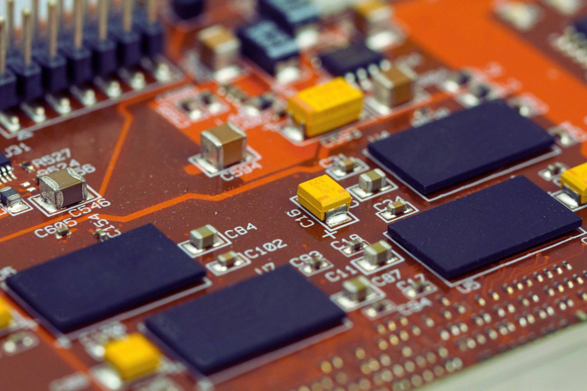
You'll typically identify an IC on a PCB as a small, black, square or rectangular package, often with many metal pins ("legs") protruding from its sides. These pins are what connect the IC to the copper traces on the PCB. Each IC usually bears a unique identifier or part number, a handy detail for cross-referencing datasheets.
The Blueprint for Brilliance: Understanding the IC Design Lifecycle (Context)
Before an IC even makes it onto a PCB, it undergoes a rigorous development process. While this article focuses on the board design, understanding the IC's journey provides crucial context for why robust board design is so critical. The design of an IC itself typically involves seven stages:
- Requirements: Defining what the chip needs to do—its speed, power budget, functions, and cost targets.
- Architecture: Mapping out the high-level structure and how major functional blocks will interact.
- Micro-architecture: Breaking down the architecture into detailed components like memory, processing units, and input/output controllers.
- Implementation: Translating the micro-architecture into actual logic gates and circuits using Hardware Description Languages (HDLs) and extensive simulations.
- Bringup: Testing the first physical prototypes of the chip in a lab environment to find any design or manufacturing flaws.
- Productization: Optimizing the IC for efficient, high-volume manufacturing, ensuring quality and consistency.
- Sustaining: Ongoing support, updates, and bug fixes throughout the IC's operational life.
Every decision made during this IC design lifecycle impacts its performance, power consumption, and thermal characteristics—all factors that must be meticulously accommodated by the PCB it will eventually inhabit. This highlights the indispensable role of careful IC board design in ensuring the full potential of these sophisticated chips is realized.
Crafting Reliability: The PCB Design Process in Detail
Effective PCB design isn't just about connecting points; it's an intricate engineering discipline that directly impacts a device's performance, reliability, longevity, and even its overall cost. A poorly designed board can lead to noise, overheating, signal loss, and costly failures, regardless of how advanced the ICs are.
Here’s a deep dive into the methodical process of creating a robust PCB:
1. Laying the Foundation: Requirements and Component Selection
The journey begins long before a single trace is drawn.
- Requirement Analysis: Start by clearly defining the device's purpose. What functions must it perform? What are its physical constraints (size, weight)? What are the power requirements, operating temperatures, and expected lifespan? These questions dictate everything that follows.
- Component Selection: With requirements in hand, you'll choose the specific ICs and other passive components (resistors, capacitors, inductors) that meet these criteria. This involves scrutinizing datasheets for voltage, current, speed, and power dissipation. Cost and availability also play a significant role. Choosing the right components upfront prevents costly redesigns down the line.
2. Mapping the Connections: Topology Planning & Schematic Design
This is where the circuit starts to take shape conceptually.
- Topology Planning: Before diving into specific connections, you'll plan the high-level "map" of how your chosen ICs will connect and how signals will flow between them. The goal is to ensure simple, reliable routing and minimize potential issues like signal interference or power drops.
- Schematic Design: Using Electronic Design Automation (EDA) tools like Altium Designer, Eagle, or KiCAD, you'll create a detailed circuit diagram, or schematic. This isn't the physical layout, but a logical representation showing every component and every electrical connection. EDA tools are invaluable here, assisting with error checking, symbol creation, and preparing for the next crucial steps.
3. Catching Flaws Early: Simulation & Verification
Before committing to a physical board, extensive virtual testing is vital.
- Simulation & Verification: EDA tools allow you to simulate the circuit's behavior. This stage is critical for identifying potential problems with signal flow, power delivery, and thermal performance before manufacturing.
- Electrical Checks: These look for common issues like shorts, opens, incorrect impedance, and voltage drops.
- Thermal Checks: These simulations predict hot spots on the board, crucial for preventing component damage and ensuring long-term reliability.
- Catching issues here saves immense time and cost compared to fixing them on physical prototypes.
4. The Physical Reality: PCB Layout & Routing
This is where the abstract schematic is translated into a tangible board design.
- PCB Layout: You'll arrange the physical components on the board. Strategic placement is key:
- Keep high-speed ICs and their associated components close together to minimize trace lengths.
- Ensure power and ground lines are as short and direct as possible.
- Allow adequate space for routing traces, especially around complex ICs, and for proper thermal management components like heat sinks.
- Routing: This involves drawing the copper traces that connect all the parts on the PCB, following the schematic. Critical rules apply:
- Avoid sharp 90-degree corners in traces, as they can cause signal reflections.
- Keep traces as short and direct as possible to maintain signal strength and reduce electromagnetic interference (EMI).
- Plan for differential pairs (for high-speed signals) and controlled impedance lines carefully.
5. Mastering the Essentials: Core Principles for Robust Boards
Beyond just connecting components, several fundamental engineering principles must be rigorously applied to ensure a board's reliability and performance.
Power Delivery (Power Integrity)
Stable and clean power is non-negotiable for ICs to operate correctly. Any voltage fluctuation or noise on the power rails can disrupt an IC's functionality, leading to errors or crashes.
- Wide Traces: Use wide copper traces for power and ground lines to minimize resistance and voltage drop.
- Decoupling Capacitors: Place these small capacitors extremely close to the power pins of every IC. They act as tiny reservoirs, providing instantaneous current to the IC during rapid switching and filtering out high-frequency noise.
- Multi-layer Designs: In complex boards, dedicated ground and power planes (full layers of copper) are often used. These provide extremely low resistance paths for power and ground, further minimizing noise and aiding heat dissipation.
Signal Integrity (SI)
Signal integrity refers to the quality of the electrical signals traveling through the PCB traces. A "clean" signal arrives at its destination without distortion, reflections, or interference, ensuring reliable data transfer.
- Short, Straight Traces: Minimize trace length and avoid unnecessary bends to reduce signal degradation.
- Controlled Impedance: For high-speed signals, traces must have a consistent characteristic impedance (resistance to alternating current). Matching this impedance across the signal path prevents reflections that can corrupt data.
- Proper Spacing: Maintain adequate spacing between adjacent traces to prevent crosstalk, where a signal on one trace induces noise on another.
- Ground Planes: Utilizing a solid ground plane beneath signal layers provides a consistent return path for current and helps shield signals from external noise.
Thermal Management: Beating the Heat
ICs generate heat, and excessive temperatures can significantly reduce their lifespan and cause performance issues. Effective thermal management is crucial for device longevity.
- Wide Copper Areas: Design large copper areas (planes or pours) around hot components to act as heat sinks, drawing heat away.
- Thermal Vias: These are small, plated holes that connect copper layers, allowing heat to transfer efficiently from hot components on one side of the board to a cooler side or internal plane.
- External Heat Sinks: For very high-power ICs, external heat sinks, sometimes coupled with fans, may be necessary. The PCB layout must accommodate these.
Electromagnetic Compatibility (EMC): Playing Nice with Others
EMC ensures that a board functions correctly in its electromagnetic environment without causing or being susceptible to unwanted electrical noise (Electromagnetic Interference, EMI).
- Minimize Loop Areas: Keep current loops (the path from source, through component, to ground) as small as possible to reduce antenna effects.
- Avoid Long Parallel Traces: This can increase crosstalk and EMI radiation.
- Shielding: Use ground planes and, in some cases, metallic enclosures to shield sensitive components or entire boards.
- Filters and Ferrite Beads: These components can suppress noise on power lines and signal paths.
Designing for Production: Manufacturability
A brilliant design is useless if it can't be efficiently and affordably manufactured. Design for Manufacturability (DFM) principles are about making the board easy for factories to build.
- Standard Part Sizes: Use readily available components to reduce sourcing complexity and cost.
- Clear Labeling: Ensure silkscreen labels are clear and correspond to component placements.
- Logical Layout: An organized, intuitive layout simplifies assembly and troubleshooting.
- Simple Routing: Avoid overly complex or tightly packed routing that can lead to manufacturing defects.
- Appropriate Via Sizes: Use standard via sizes and avoid extremely small ones unless absolutely necessary, as they increase manufacturing cost and complexity.
6. Bringing It to Life: Manufacturing & Testing
The design culminates in physical production and verification.
- Manufacturing: You'll prepare detailed production files (Gerber files for layers, drill files, assembly drawings). Fabrication involves etching copper traces, drilling holes, applying solder masks, and silkscreen printing. Quality control checks are performed at various stages.
- Post-Production Testing: Once manufactured, the physical boards undergo rigorous testing:
- Functional Testing: Verifying the board performs its intended operations.
- Signal Integrity and Power Delivery Checks: Ensuring signals are clean and power is stable.
- Thermal Performance: Monitoring actual temperatures under load.
These checks ensure the final product meets design specifications before mass production begins.
Beyond the Basics: Evolving Trends in Board Design
The world of electronics is constantly evolving, and PCB design is no exception. Engineers must stay abreast of new technologies that allow for smaller, faster, and more robust devices.
Stacking Up: The Power of Multilayer Boards
Gone are the days when most boards were single-sided. Modern complex devices rely heavily on multilayer boards, which stack multiple layers of copper traces separated by insulating material.
- Benefits: This technology allows for far more circuits in a smaller footprint, drastically improves signal paths (by allowing dedicated high-speed layers), reduces interference (with internal ground and power planes), and enhances power delivery. They are essential for today's complex, high-speed devices like computers and advanced networking equipment.
More in Less Space: High-Density Interconnect (HDI)
As devices shrink, the need to pack more connections into less space becomes critical. High-Density Interconnect (HDI) boards address this by utilizing very thin lines and spaces, smaller vias (microvias), and sometimes even laser-drilled blind and buried vias.
- Benefits: HDI enables lighter, thinner devices with superior electrical performance, capable of handling fast signals and quick data transfers more effectively. Often combined with multilayer boards, HDI is found in smartphones, tablets, and wearable electronics.
Bending the Rules: Flexible PCBs
Traditional PCBs are rigid, but for many applications, flexibility is key. Flexible PCBs are made from thin, pliable plastic substrates (like polyimide) with copper traces laminated onto them, allowing the boards to bend and twist without breaking.
- Benefits: Ideal for wearables, medical devices, cameras, and products requiring unique form factors or fitting into tight, irregular spaces. They reduce weight, simplify assembly by eliminating connectors, and improve reliability in dynamic environments.
Speed Demons: RF and High-Speed Technology
With the proliferation of wireless communication and ultra-fast data processing, RF (Radio Frequency) and high-speed technology in PCB design has become a specialized necessity. Devices like smartphones, Wi-Fi routers, and 5G infrastructure demand meticulous design.
- Requirements: This area demands special low-loss materials, extremely precise controlled impedance traces, very short signal paths, and robust ground planes to manage fast signals without significant loss or degradation. Minimizing noise, crosstalk, and ensuring proper antenna impedance matching are paramount.
Staying Ahead of the Curve: Continuous Improvement
The electronics industry is dynamic, with new components, materials, and design methodologies emerging constantly. For any serious practitioner, continuous learning isn't just a suggestion; it's a professional imperative.
Engineers must actively seek out knowledge regarding:
- New Materials: Advancements in substrate materials that offer better thermal performance, higher frequency characteristics, or greater flexibility.
- Tools and Software: Regular updates to EDA tools bring new features, better simulation capabilities, and improved automation.
- Safety and Compliance: Staying current with international safety standards (e.g., UL, CE) and environmental regulations (e.g., RoHS, REACH).
Furthermore, the adoption of advanced methods like 3D modeling for component fitting, automated design rule checks, and even machine learning-driven layout optimization helps engineers predict and prevent design issues earlier, significantly reducing development cycles and improving product quality. This proactive approach ensures that today's designs are not just functional, but also resilient and future-proof.
Common Questions on IC Board Design
What's the biggest challenge in modern IC board design?
The increasing complexity and speed of ICs are the biggest challenges. As clock speeds rise and components shrink, issues like signal integrity, power integrity, and thermal management become exponentially harder to control. Miniaturization also means less physical space to implement solutions, pushing the boundaries of multilayer and HDI technologies.
How important are EDA tools in PCB design?
EDA (Electronic Design Automation) tools are absolutely indispensable. They are the backbone of modern PCB design, allowing engineers to schematic capture, simulate, lay out, route, and verify complex boards. Without them, designing advanced multi-layer boards with high-speed signals would be practically impossible, turning a methodical process into an error-prone nightmare.
Can I design my own PCB as a hobbyist?
Absolutely! While professional IC board design for commercial products is highly complex, hobbyists can certainly design their own PCBs. Tools like KiCAD (open source) or Eagle (freemium) offer robust capabilities for creating simpler, single or double-layer boards. It's a fantastic way to learn hands-on about electronics principles and bring your projects to life. Start with simple circuits, follow best practices, and use online resources to guide you.
Your Next Step in Electronic Excellence
The journey into the fundamentals of IC board design reveals a critical layer of engineering that powers our modern world. From defining initial requirements to meticulously routing traces and managing thermal loads, every step is a testament to precision and forethought.
Whether you're an aspiring engineer, a seasoned professional, or simply curious about what makes your gadgets tick, understanding these principles equips you with invaluable insight. The ability to translate a functional concept into a reliable, manufacturable circuit board is a skill that continues to drive innovation. By mastering these core tenets and staying updated on evolving technologies, you contribute to the creation of more efficient, powerful, and dependable electronic devices for the future.